This week we're learning about PCB fabrication, making our own pcb design come to life, and characterizing our Milling Machine.
Requirements
- Characterize the design rules for your in-house PCB production process: document feeds, speeds, plunge rate, depth of cut (traces and outline) and tooling.
- Document the workflow for sending a PCB to a boardhouse
- Document your work to the group work page and reflect on your individual page what you learned
Group Assignment
Individual Assignment
- Make and test a microcontroller development board that you designed.
Softwares 💻
- KiCAD
- MODS
- GIMP
- Arduino IDE
Group Assignment
When I first used the Milling machine to make a pcb two years ago, It was an overwhelming experience. Since then I used the milling machines many times, making other's pcbs but never my own very neat and "complicated" pcb. I once designed and fabricated a simple pcb with THT components: with a battery and LED and designed it with KiCad as well.
But it's gentlemen! It's time to make something fancy and to get good to soldering!
Characterizing Our Milling Machine
In this week, we're gonna use our CNC Milling machine called "China Router", but first What we mean when we talk about "characterizing the machine"?
This refers to the maximum clearance of each copper trace can be milled on the machine can mill and the maximum clearnace bewtween traces. This is waht factors in choosing our routes in our PCB design software. And these parameters are placed in the "Design Rules" in Kicad for example.
To begin the machine need surfacing so we performed a surfacing operation from OpenBuildsControl's Wizard.
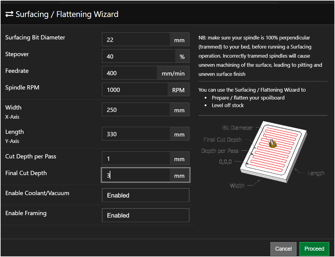
After surfacing
After making sure the bed is leveled, we downloaded the clearance test from FA site and went ahead to mods. The o.oo1 area wasn't smooth.
Output
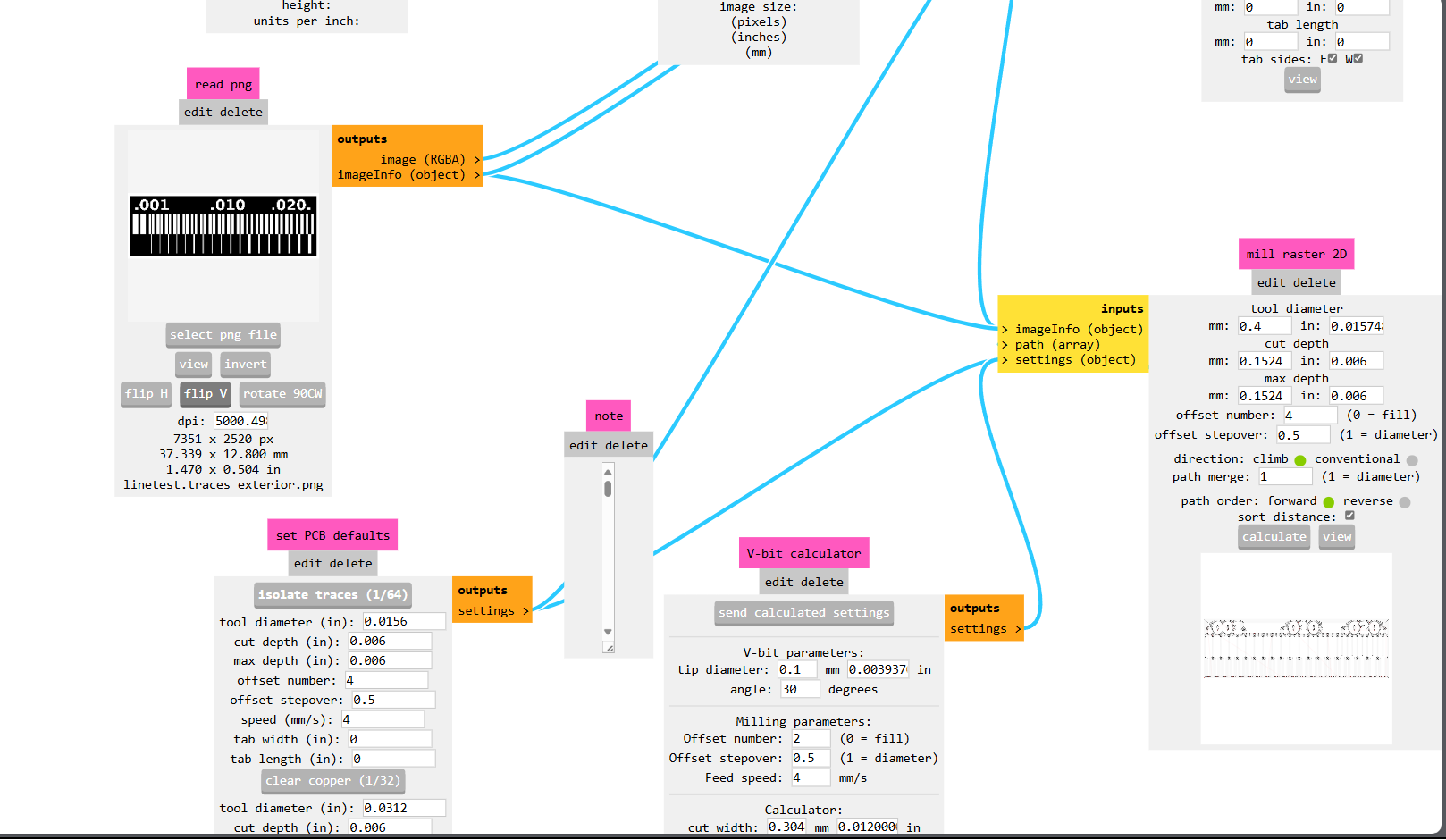
workflow for sending a PCB to a boardhouse
Check out our group documentation.
ESP32 board
After the lecture I revisited the first video I watched about soldering by the lovely Doaa from 2021 Student Bootcamp. Then I went to watch extra resources to help me with solderng SMD components. This is an old but gold video by Collin's Lab. I already decided to fabricate the board I designed in week 6. I only needed some pretifying for the schematics.
Components PCB
My components are listed in week 6's page . I used the same components but I added 2 Zero ohm resistors that can act as bridges.
PCB Design in KiCad
I used the same design but modified some things.
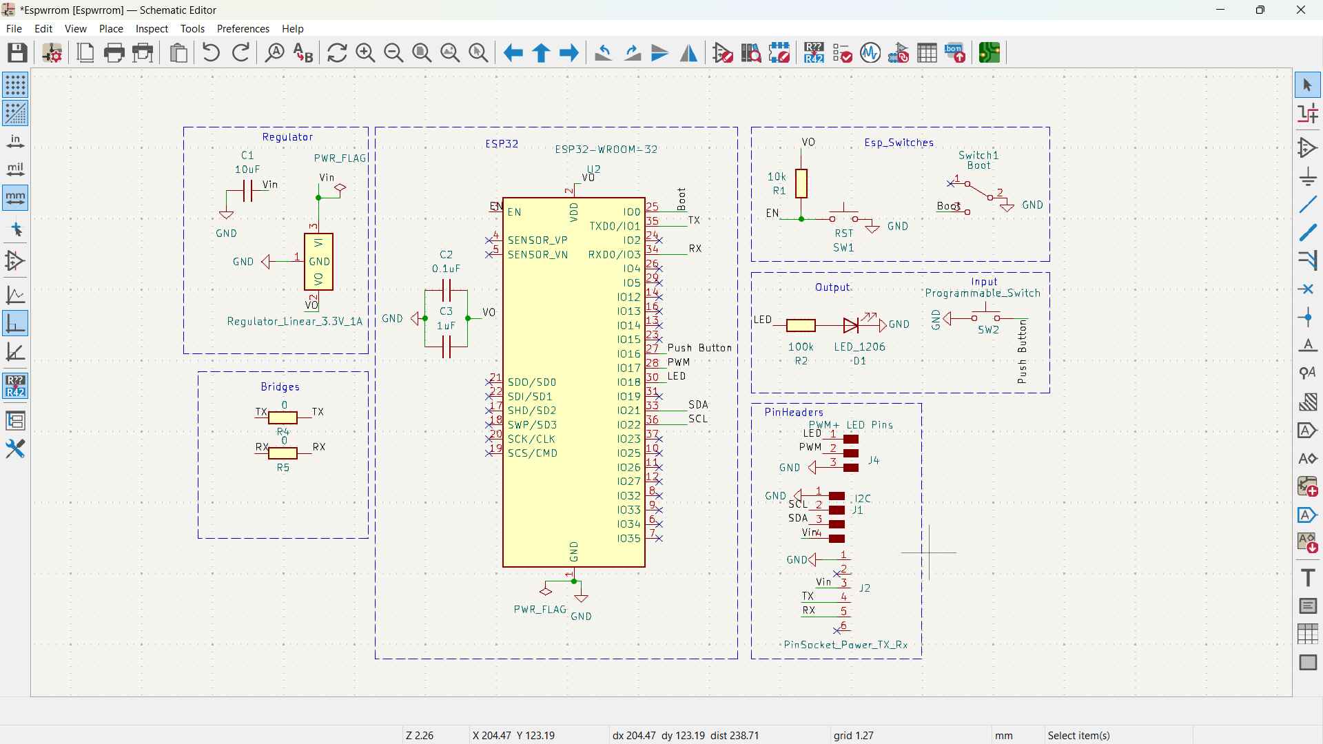
Schematic
After I made the things a bit neater I added the 0 ohm resistors in put them is rectangle with the name "Bridges". I like to arrange by functionality in my schematics.
Layout
I had some comments from fellow instructors about my pcb design so I tweaked the design a little bit to make room for the Esp's antenna for example.I had an issue with the DRC of unconnected traces and I couldn't find a way to connect them. Then someone recommended that I use the 0 ohm resistors as bridges and re-routed. Once done, I exported the Gerber Files was ready to go.
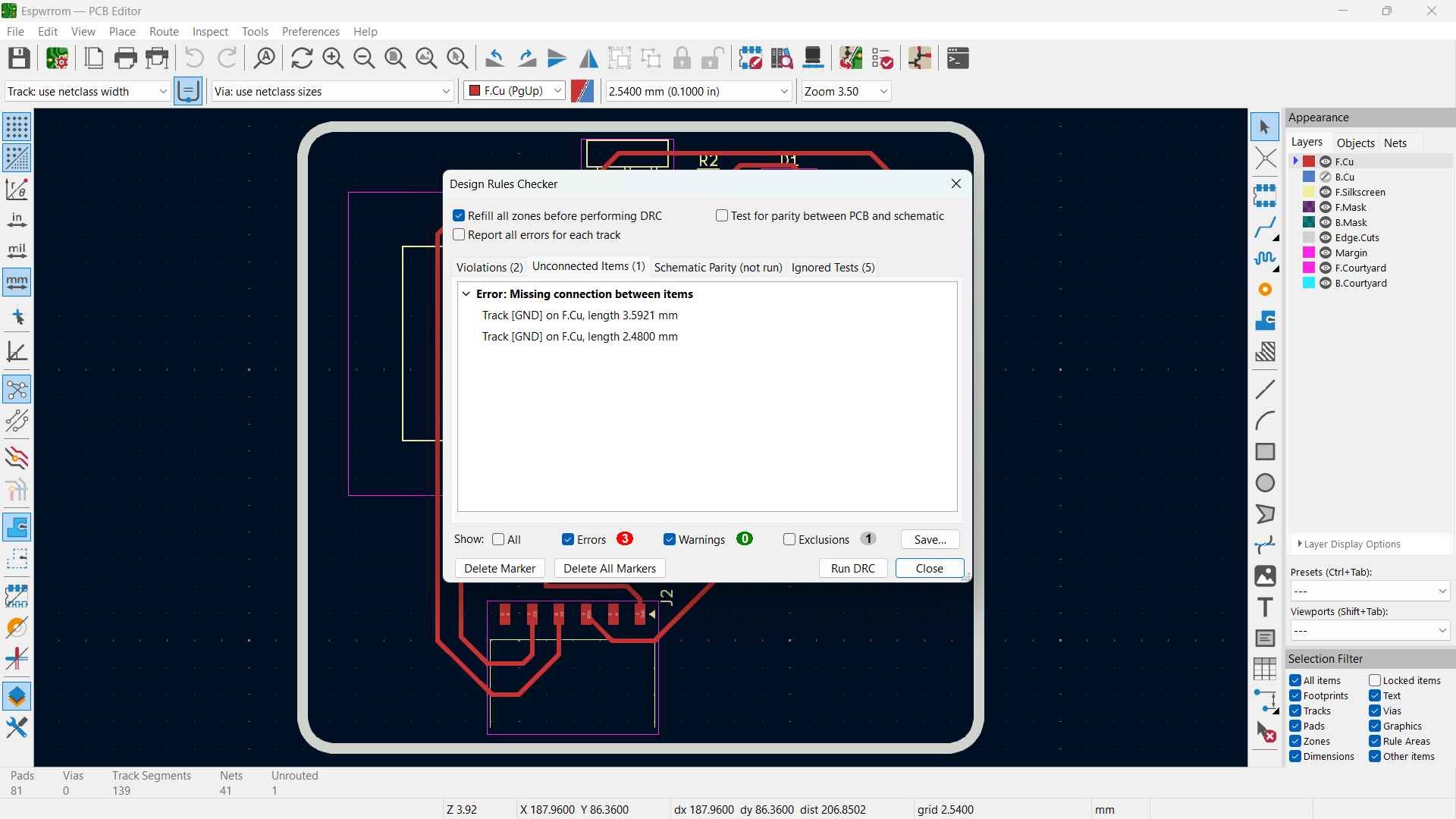
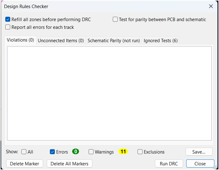
DRC
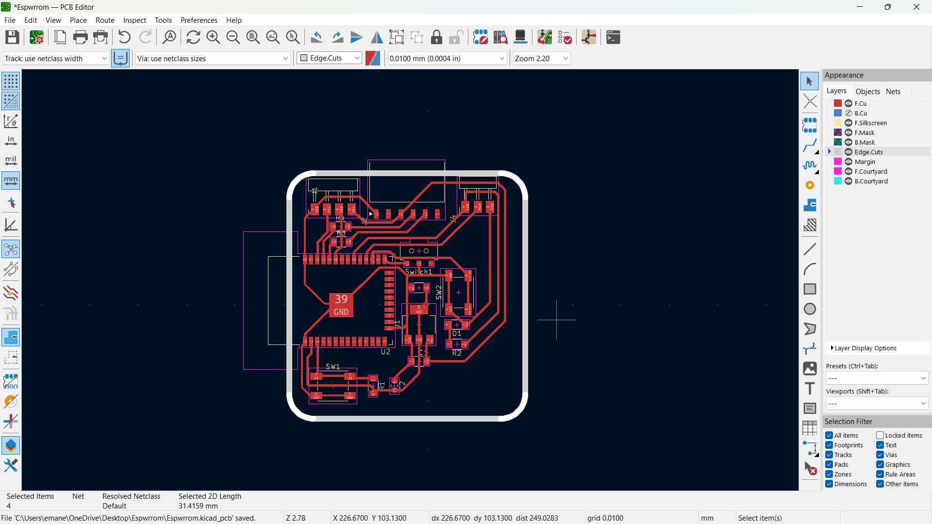
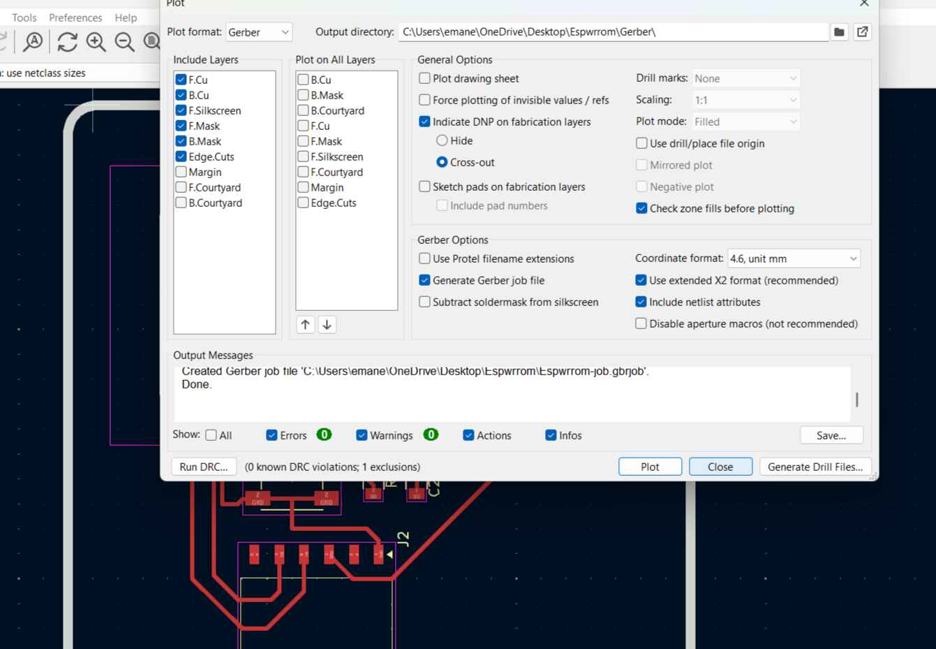
Fabrication
Gerb viewer & Gerbv
I used Gerb Viewer to measure the pcb's dimensions and try to export png. my pcb is 6.5 by 5.5 cm^2 and it only exported PDF. It also gave a lot of spacing around the pcb itself and after discussion about if this would be a problem or not, I decided to go back to trustee Gerbv to export the png.
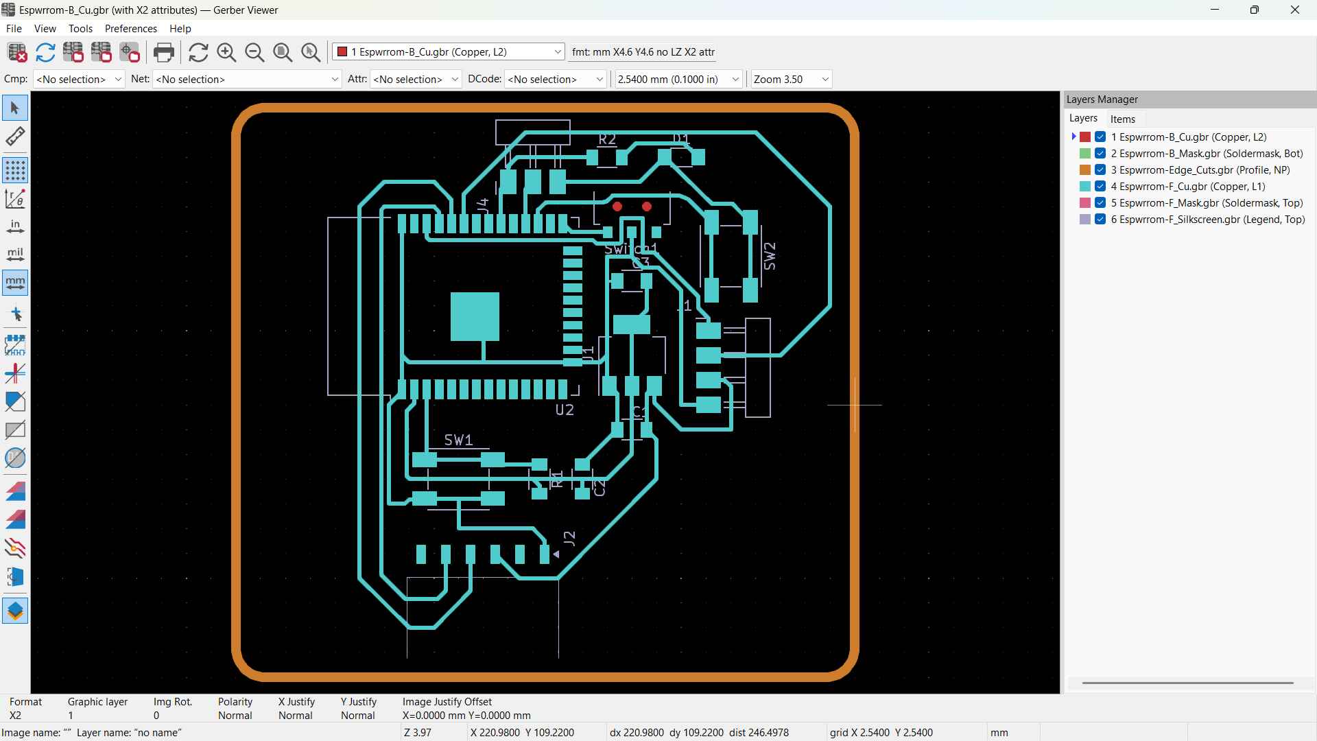

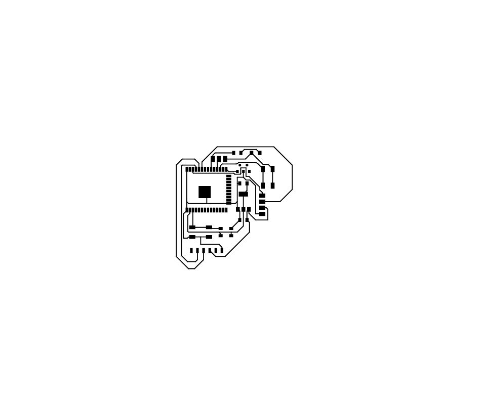
Gerbiewer PDF view
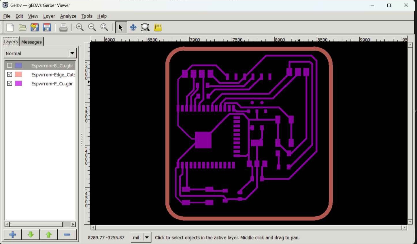
Gerbv
I checked edge cuts and traces layers and unchecked the bottom layer, then made them black and used maximum opacity. Once done I exported the outline alone then the traces with the outline
GIMP
To prepare the png for mods and milling, the photos need to be only black and white and of certain quality. This cannot be done in gerbv. We typically use GIMP. Once we open the design in GIMP, I made the resolusion 1000. Then Image> Mode> Indexed> Black & white, from Color tab> Value Invert, and finally fill the outline black we'll not need it. The same procedure is done for the outline excluding the value invert and we fill the outside of the outline with black.
The machine only sees black and white: white for traces and black for the outline or drills if present. Finally we can export the png!
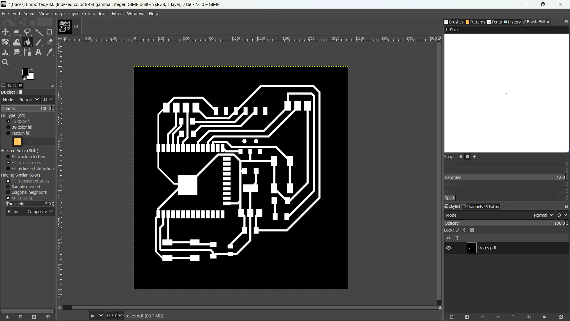
Mods
In Mods I imported the png select the mode to be isolate traces, leave the offset to be 4 and change the dimaeter of the tool to be 0.3mm
We do the same for the outline but choose the "mill outline" button and change the diameter of the cutting tool.
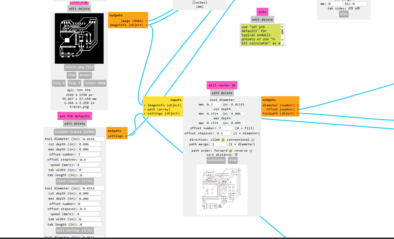
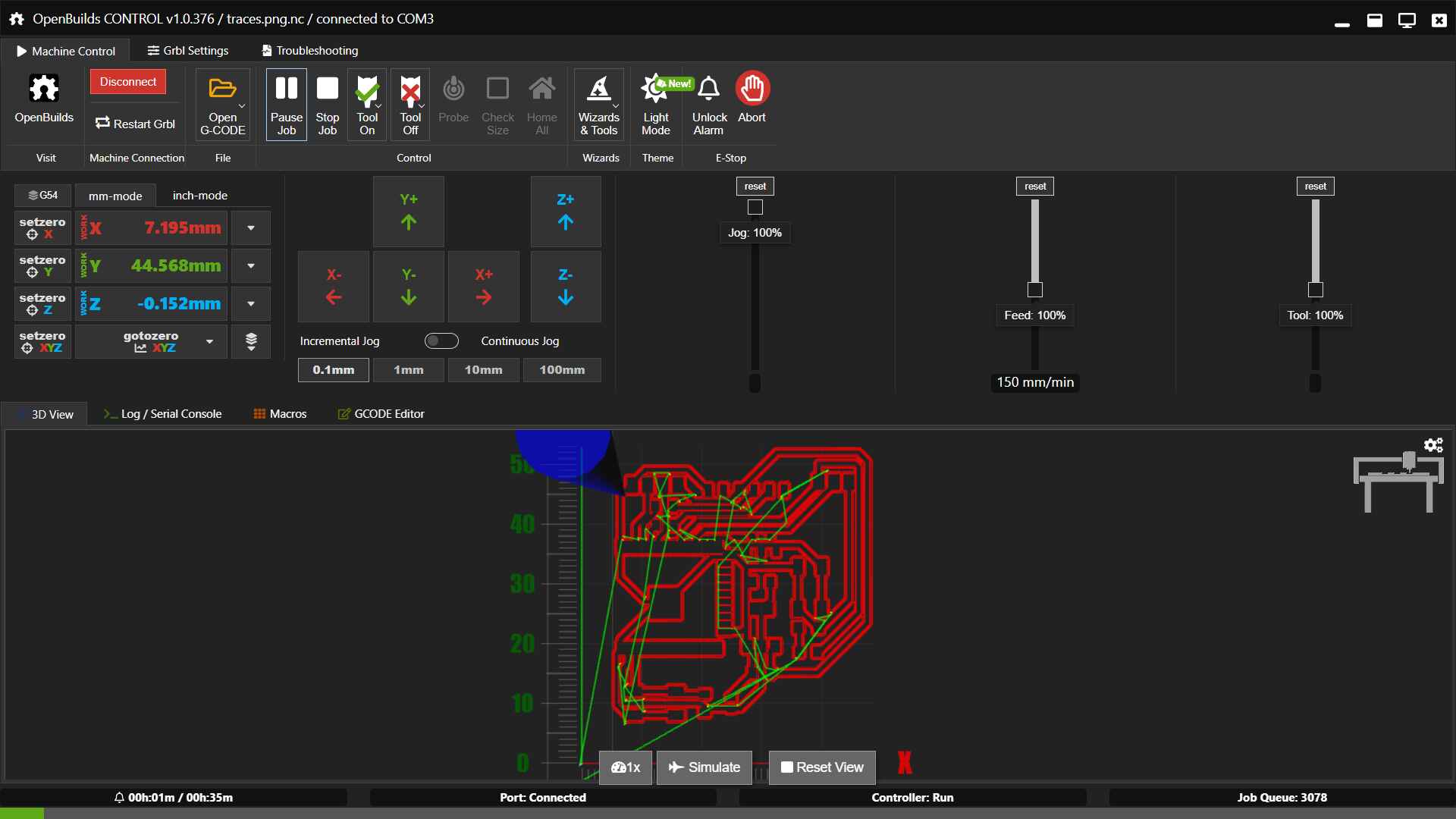
OpenBuilds Control
PCB
I didn't like the traces and how it looks. I think was the cause is using a 0.4 endmill while choosing o.3 in Mods because the esp32 pads are less than 0.4mm and we didn't have the 4mm collet to fit the shank of the 0.3 endmill. I used the multimeter and checked continuity for each trace and all seemed fine. so I went ahead and soldered the components.
Soldering & testing
I had a lot trouble soldering the teeny-tiny components but I managed to solder them with Lead-free soldering wire and a lot of patience.
programming
We tried running a blinking code on the ESP but it didn't upload and I discovered I mixed TX, RX connection is not correct. We used male-female jumper to extend the connection and rearrange the rx-tx and it uploaded. But the blinking was faint so I discovered I needed a smaller resistor value.. well boy oh boy the more you learn
ESP32 board v2
I wanted to make an iteration to the pcb so I added a power LED & Fixed my assigned resistor value. Here's the updated schematic and layout.
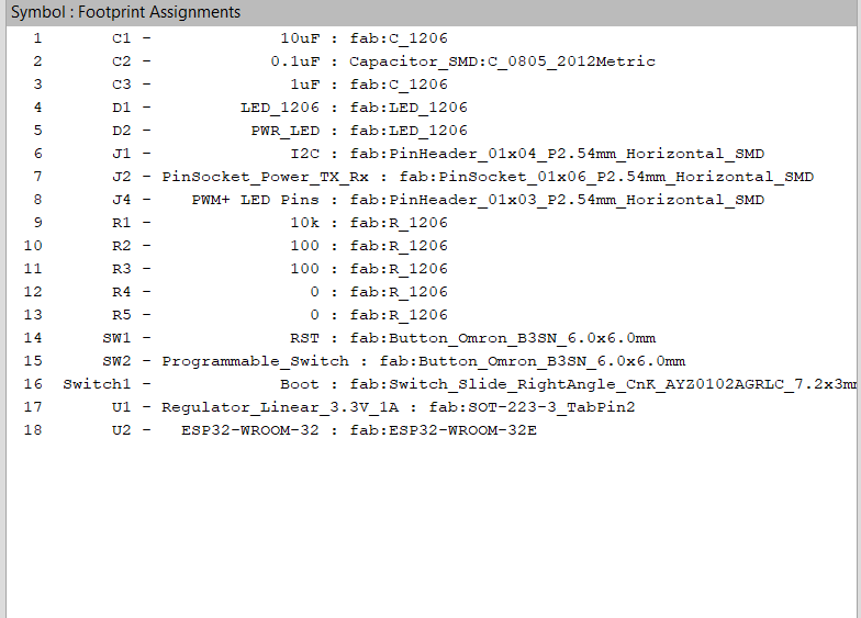
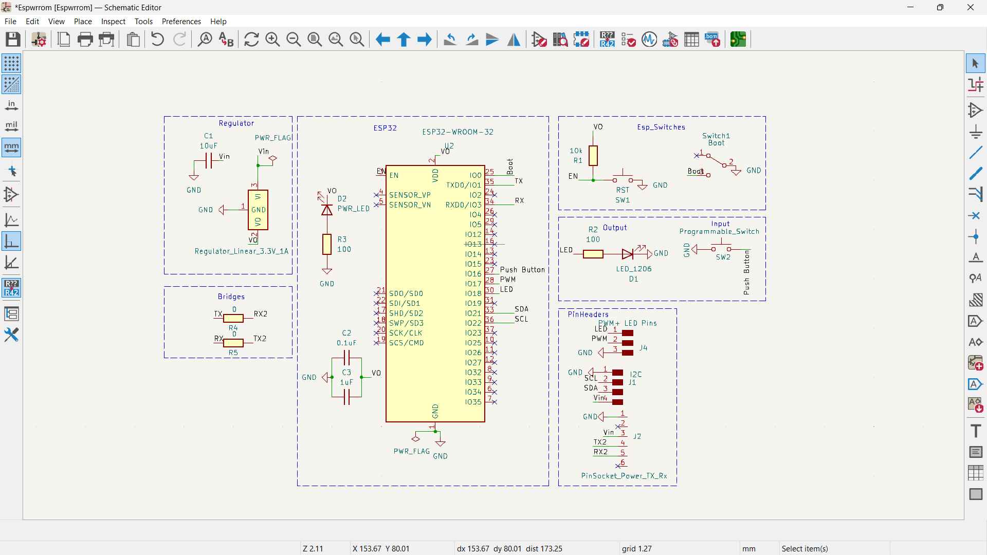
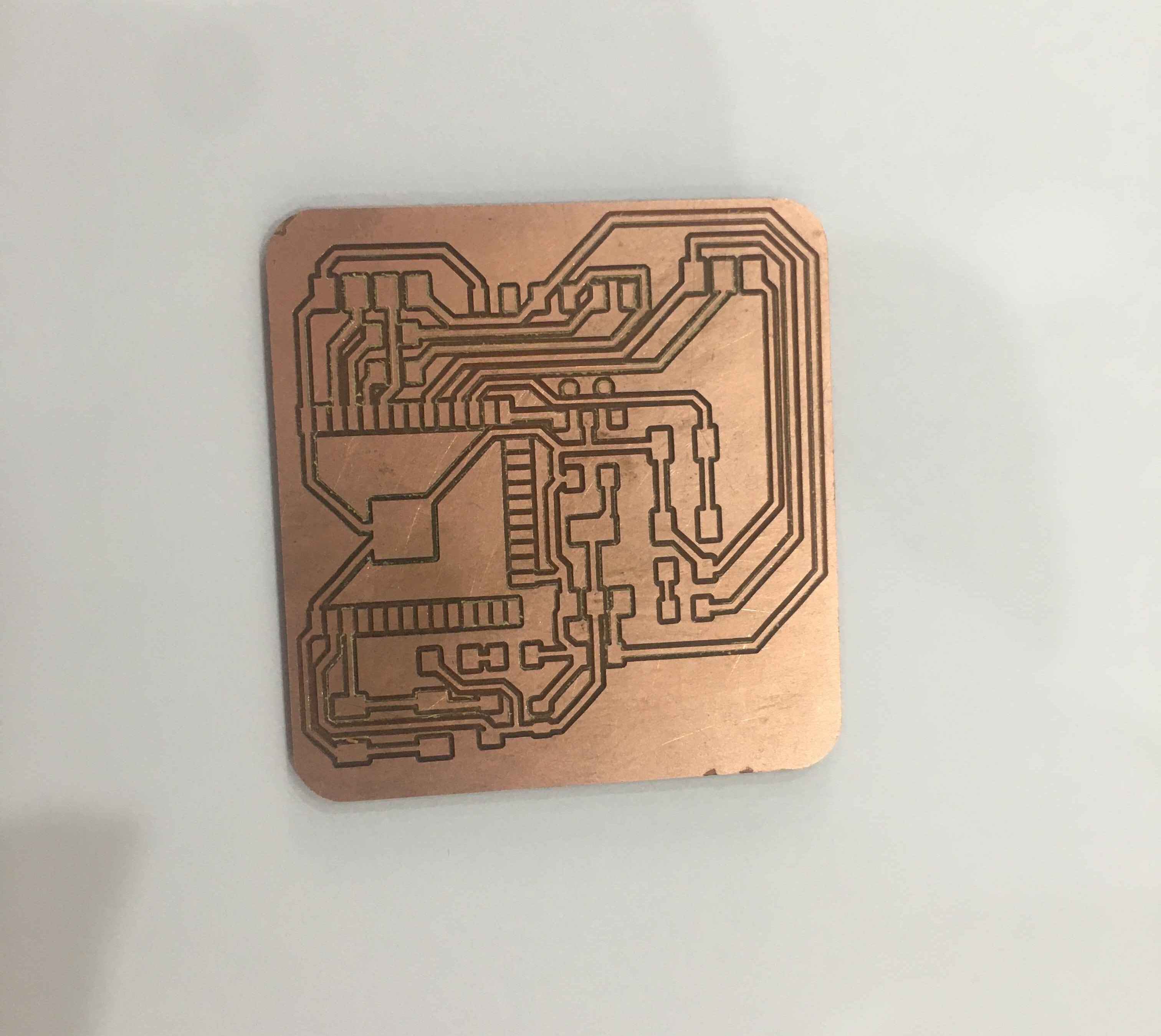
In the fabrication phase I used a 0.3 endmill, once it was provided by our fab lab.
I turned out very clean! I'm proud and It actually works!!
The Code
              void setup() {
                pinMode(16, INPUT_PULLUP);
                pinMode(18, OUTPUT);

                Serial.begin(115200);
              }

              void loop() {
                int push = digitalRead(16);
                if(!digitalRead(16)){
                  digitalWrite(18,HIGH);
                }
                else
                {
                  digitalWrite(18,LOW);
                }

                delay(50);
              }